產品介紹
陶瓷散熱基板 薄膜製程
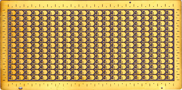
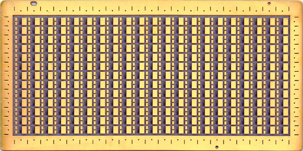
DPC, direct plate copper, applies techniques in semiconductor thin film process. Various metal circuits and fine trace patterns can be manufactured on the surface of ceramic substrate.
By integrating the heat-dissipation ability of ceramic and the conductivity of metal, ceramic substrate consists of various superior physical properties. The composite thin film process increases the adhesion strength, dimension accuracy and smoothness of circuit trace.
Applications
- 1. High Power LED Package Substrate
- 2. Solar Cell
- 3. Hybrid Electric Vehicles
- 4. Microwave (Wireless Communication)
- 5. Semiconductor Process Equipment
Substrate Physical Properties:
| Characteristic Value | AlN | Al2O3 (96%) |
|---|---|---|
| Color | Gray | White |
| Density | 3.3 g/cm3 | 3.7 g/cm3 |
| Thermal Conductivity | ≧170 W/mk | ~22 W/mk |
| Coefficient of Thermal Expansion | 4.6 x 10⁻⁶/℃ (R.T.~400℃) | 7.3 x 10⁻⁶/℃ (25~800℃) |
| Dielectric Strength | 15 KV/mm> | 14 KV/mm (AC 60Hz) |
| Volume Resistivity | ≧1013Ω‧cm | ≧1014Ω‧cm (25℃) |
| Dielectric Constant | 9.0 1MHz | 9.4 1MHz |
| Bending Strength | ≧330 MPa | ≧320 MPa |
Specification
| Characteristic | ALN | Al2O3 (96%) | |
|---|---|---|---|
| Substrate Part | Dimensions | Up to 4.5” x 4.5” | Up to 5” x 5” |
| Dimensional Tolerance | ±1% NLT ±0.1mm | ±0.60%, NLT : ±0.08mm | |
| Thickness | 0.38 / 0.5 / 0.635 mm | 0.38 / 0.5 / 0.635 / 1.0 mm | |
| Thickness Tolerance | ±10% > | ±10.0%, NLT : ±0.05mm | |
| Metalized Part | Conductive Layer | Cu-Ni-Au / Cu-Ni-Ag / Customized Up to 100μm in Thickness |
|
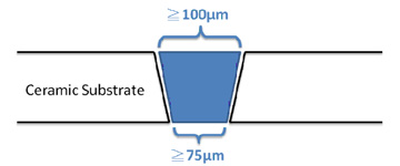
| Via Hole | φ75μm min | ||
| Pattern Construction | Single Face / Double Face with Via Holes / Customized | ||
Tel: +886 2 8792-1266
Fax: +886 2 8792-1266
Address: 9F., No. 136, Sec. 2, Keelung Rd., Da’an Dist., Taipei City 106, Taiwan (R.O.C.)
群尚科技有限公司 © 2019 Soar Technology Co., Ltd. All Rights Reserved.